A little over a year ago (I'm writing this on 2/15/2024, so this must be 2023 or 2022), I started learning about how to "decap"
the chips from integrated circuits using a method that I found on YouTube. The method is to use a hot air gun to heat up the IC
and then, as the YouTuber put it, it will "break like a bar of chocolate." If you hold the IC just right with a couple pairs of
pliers, the crack will go over the center of the chip, and it will fall right out of the plastic casing. At this point, you just
yank the little wires from the pins and you're left with a little silicon wafer full of thin shiny traces.
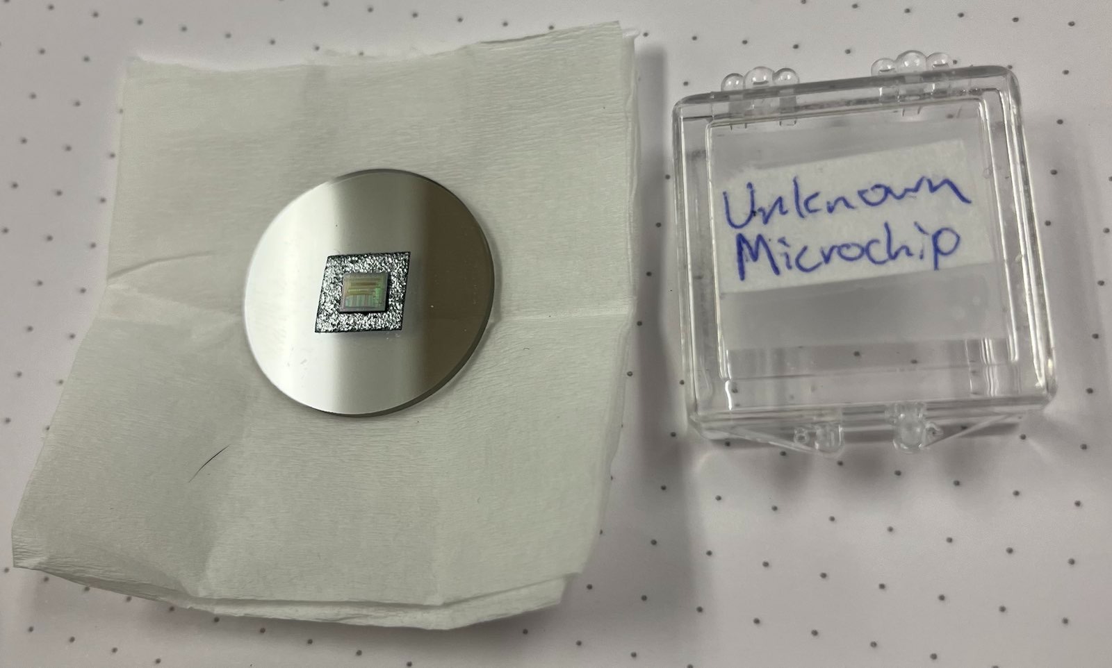
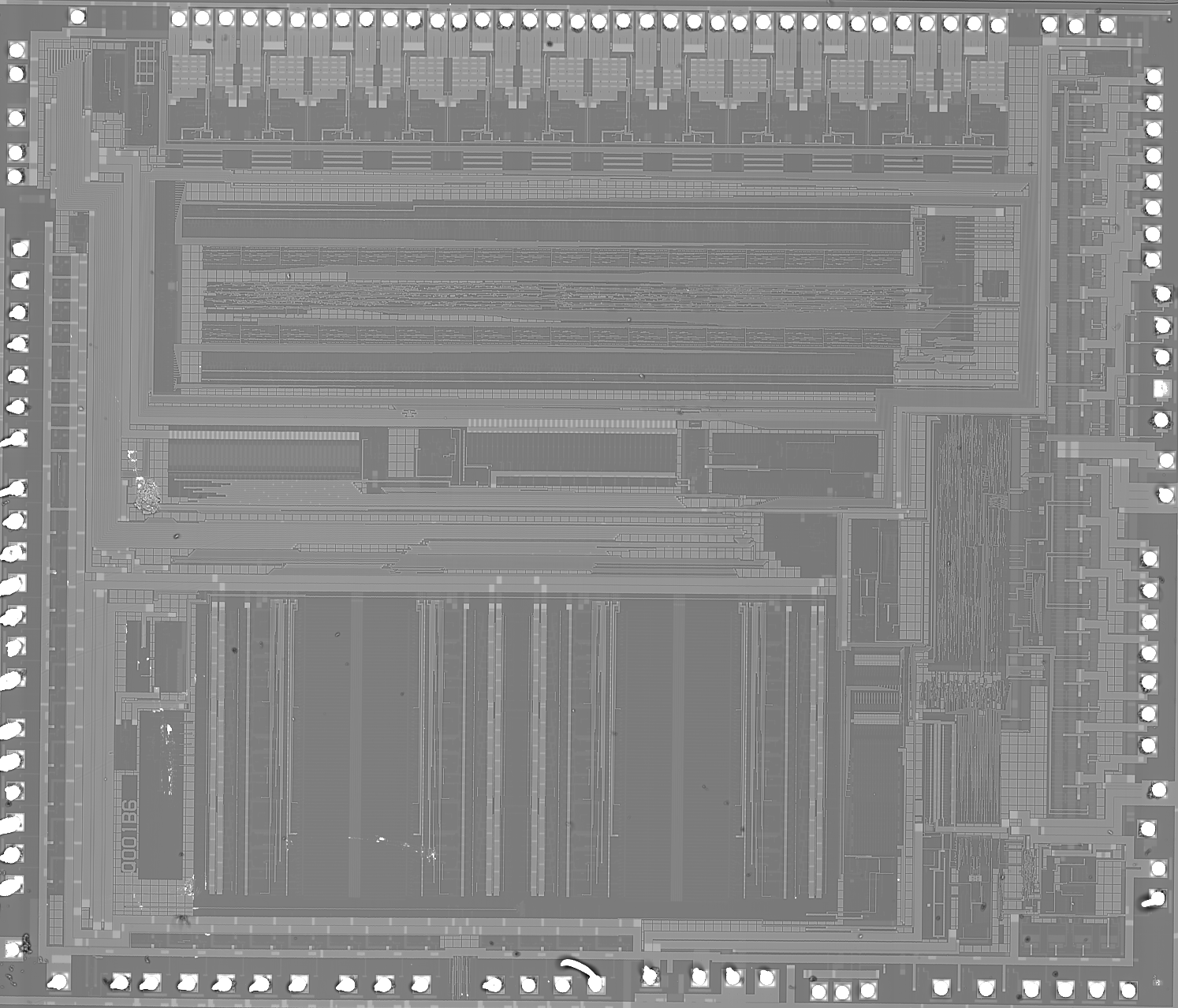
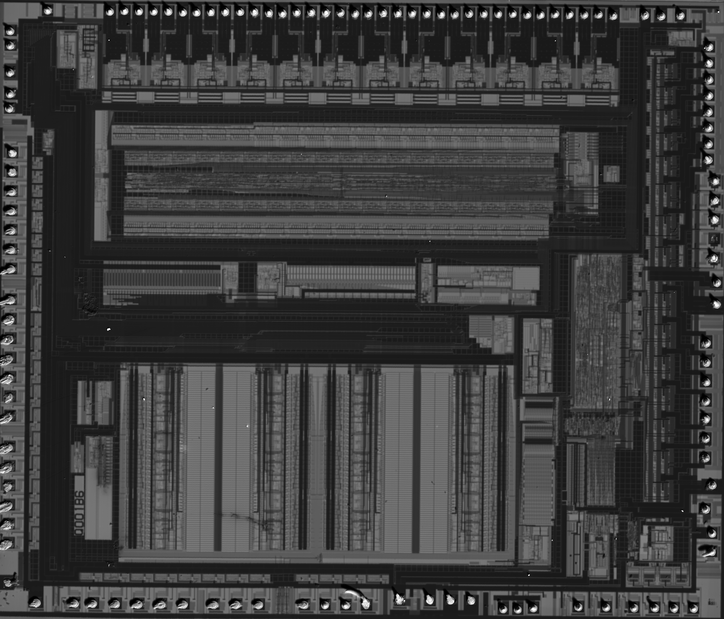
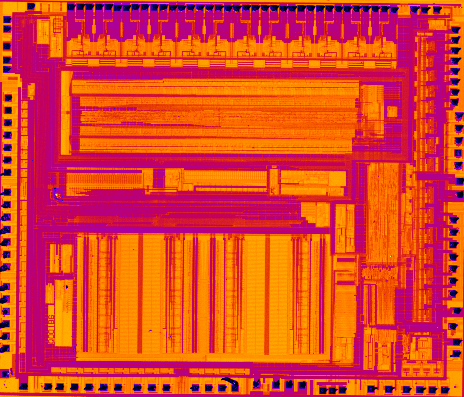
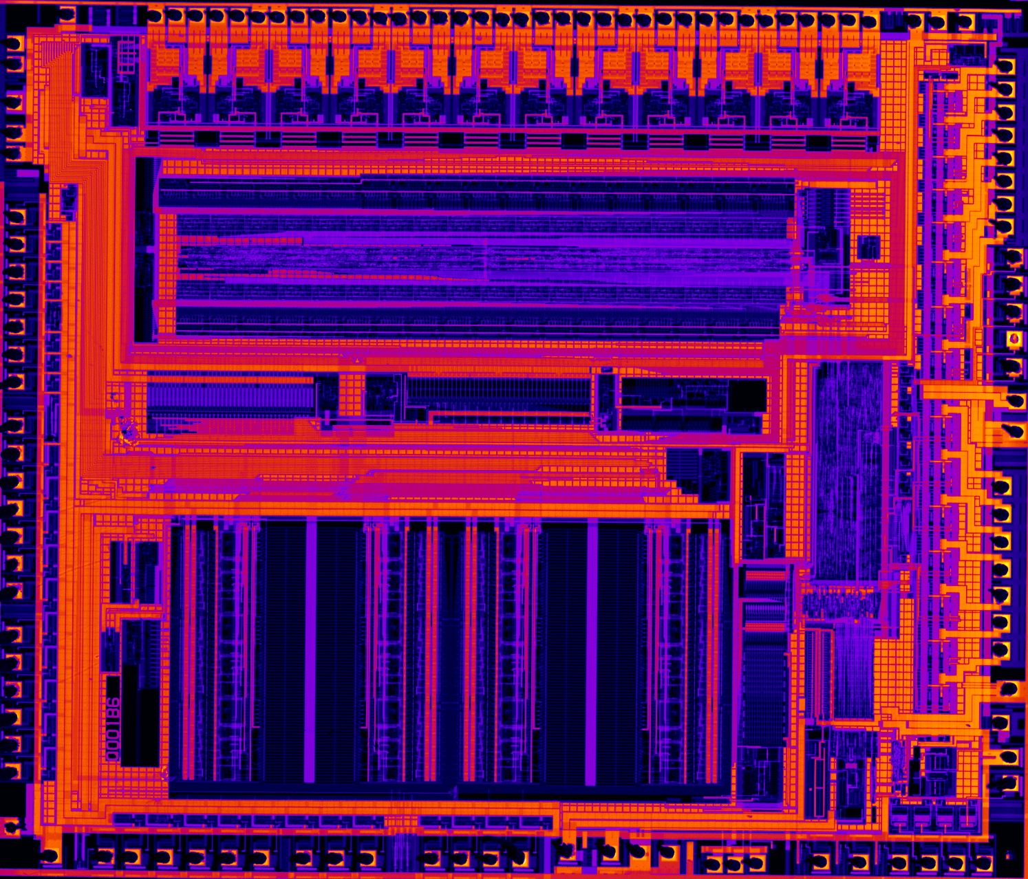
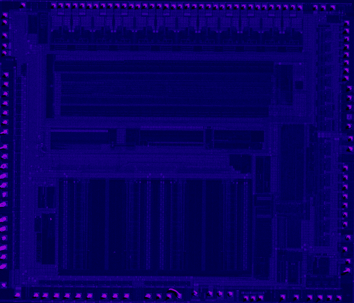
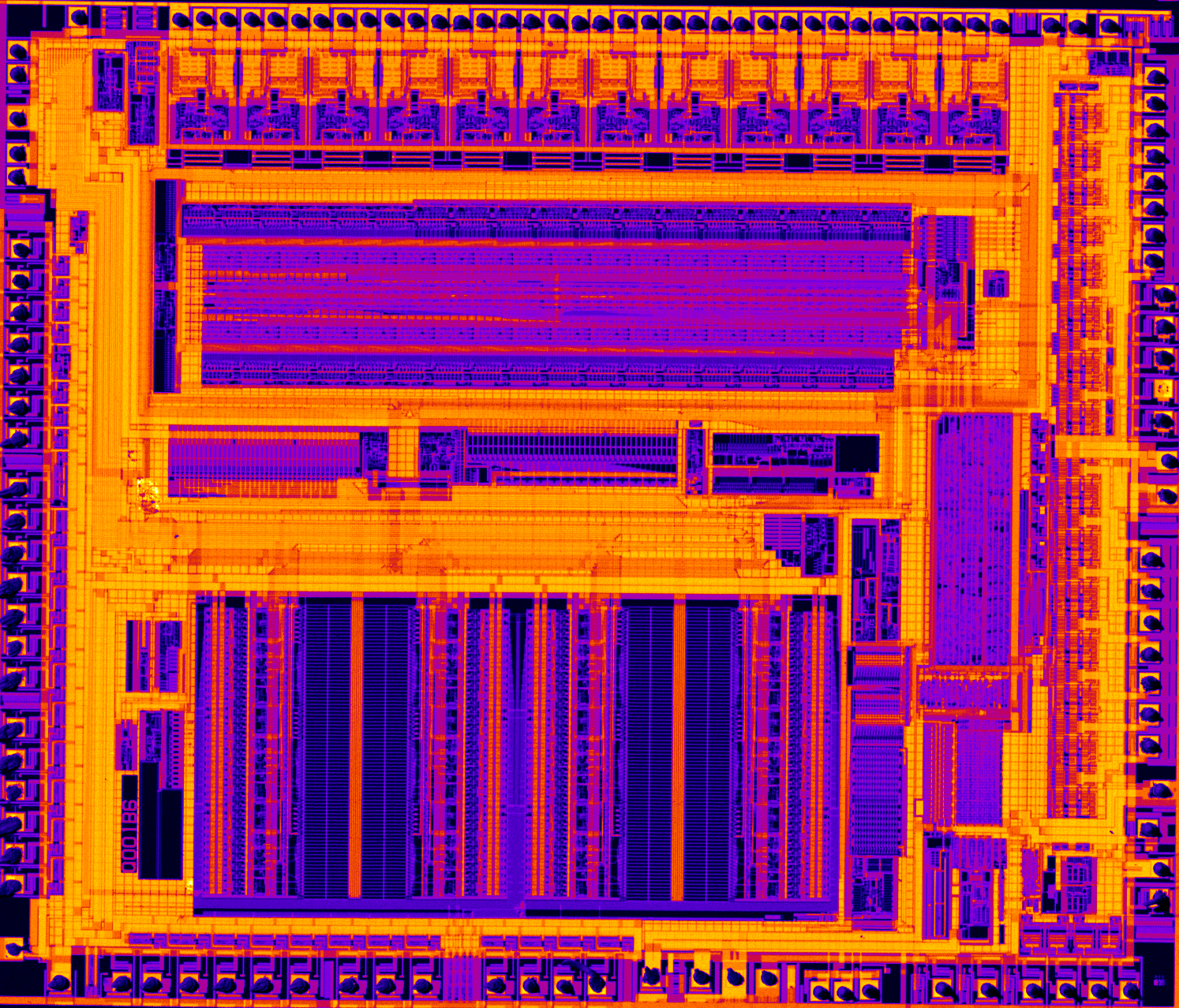
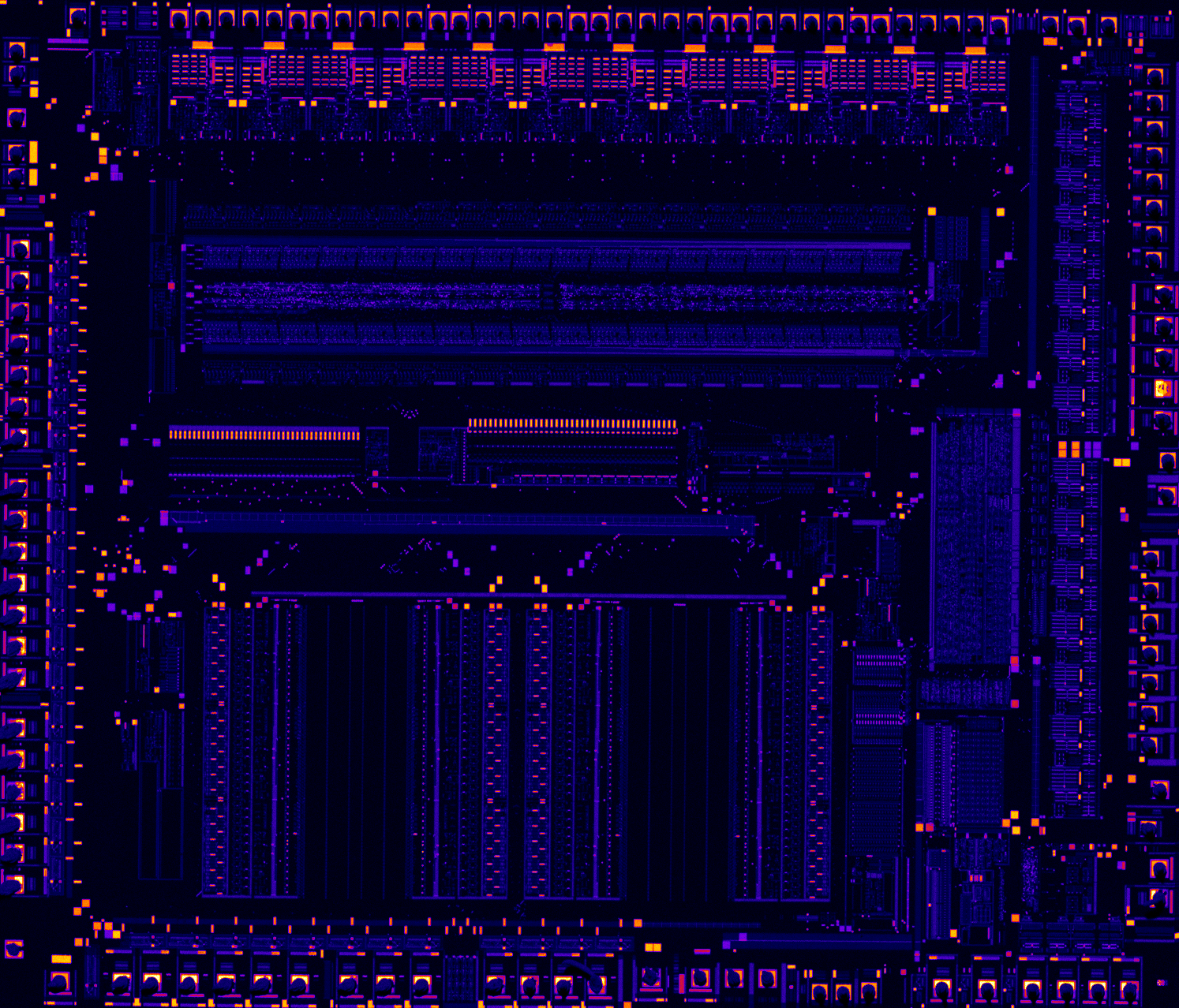
240215 -- Photo of unknown microchip sample taken with my phone. The sample has been carbon coated.
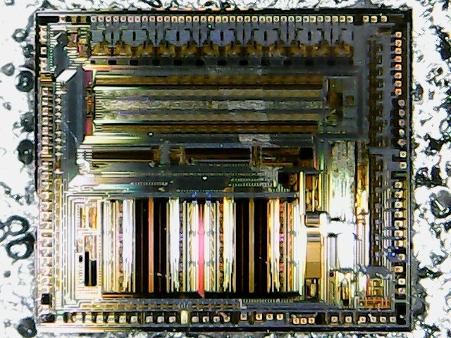
240215 -- Photo of unknown microchip sample taken with a low-powered, cheap USB microscope. It's hard to see the traces
using this camera without creating too much glare from the light source on the camera. The exploratory microprobe analyses
I did today are from the lower right part of the chip as viewed in the image.
I've recently been learning about methods for analyzing thin films using EPMA, so I think this sample may provide a good test
case to develop these methods.
As I understand it, thin films are analyzed using point analyses. It's clear from looking at the IC briefly that there are traces
going all over the place, and it's not immediately clear to me what they are made of or which ones might be detectable within the
analytical volume of an analysis and which are too deep to detect below the surface. The first thing to try will probably be mapping
the sample using WDS over whatever area that time permits. However, I need to figure out which elements to map first.
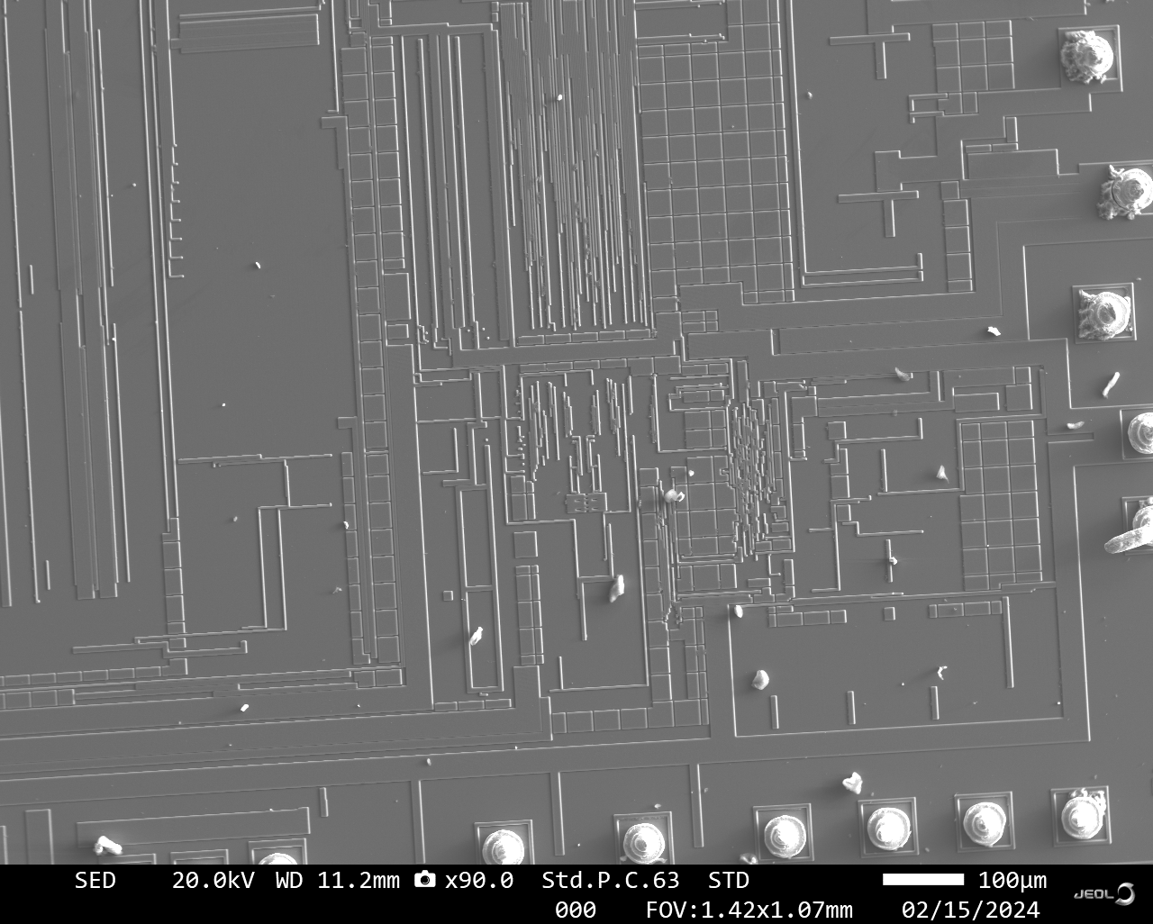
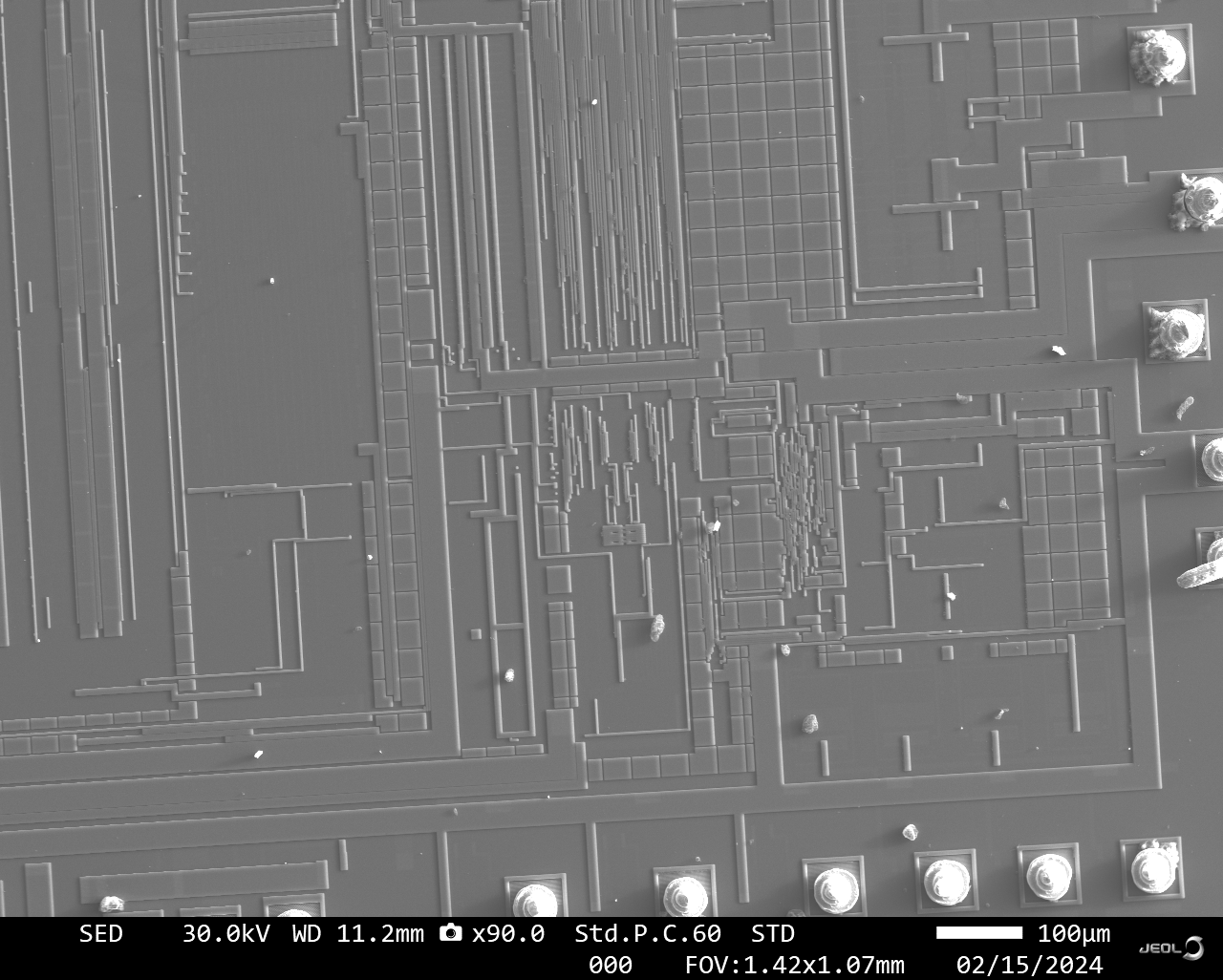
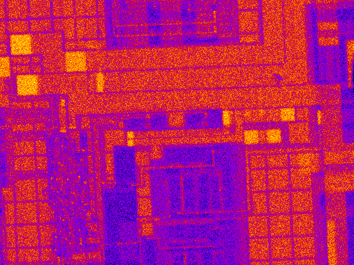
240215 -- SED image of ROI at 20 kV and 30 kV accelerating voltage. It appears that the dust particles are slightly more
transparent and some of the "buried" traces are slightly more visible at the increased voltage.
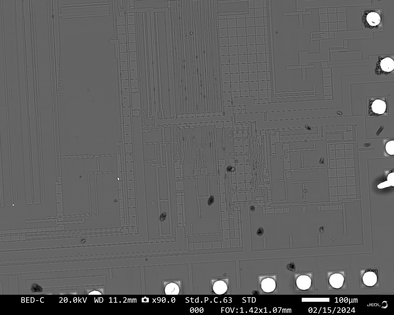
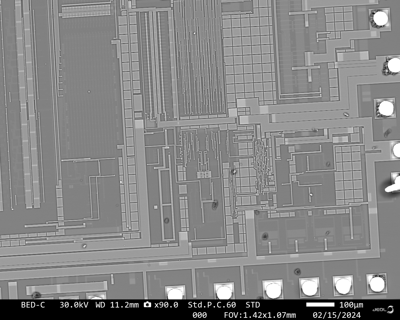
240215 -- BED-C image of ROI at 20 kV and 30 kV accelerating voltage. The "buried" traces are WAY more visible at 30 kV.
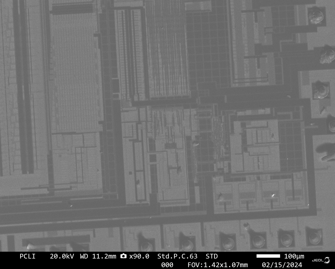
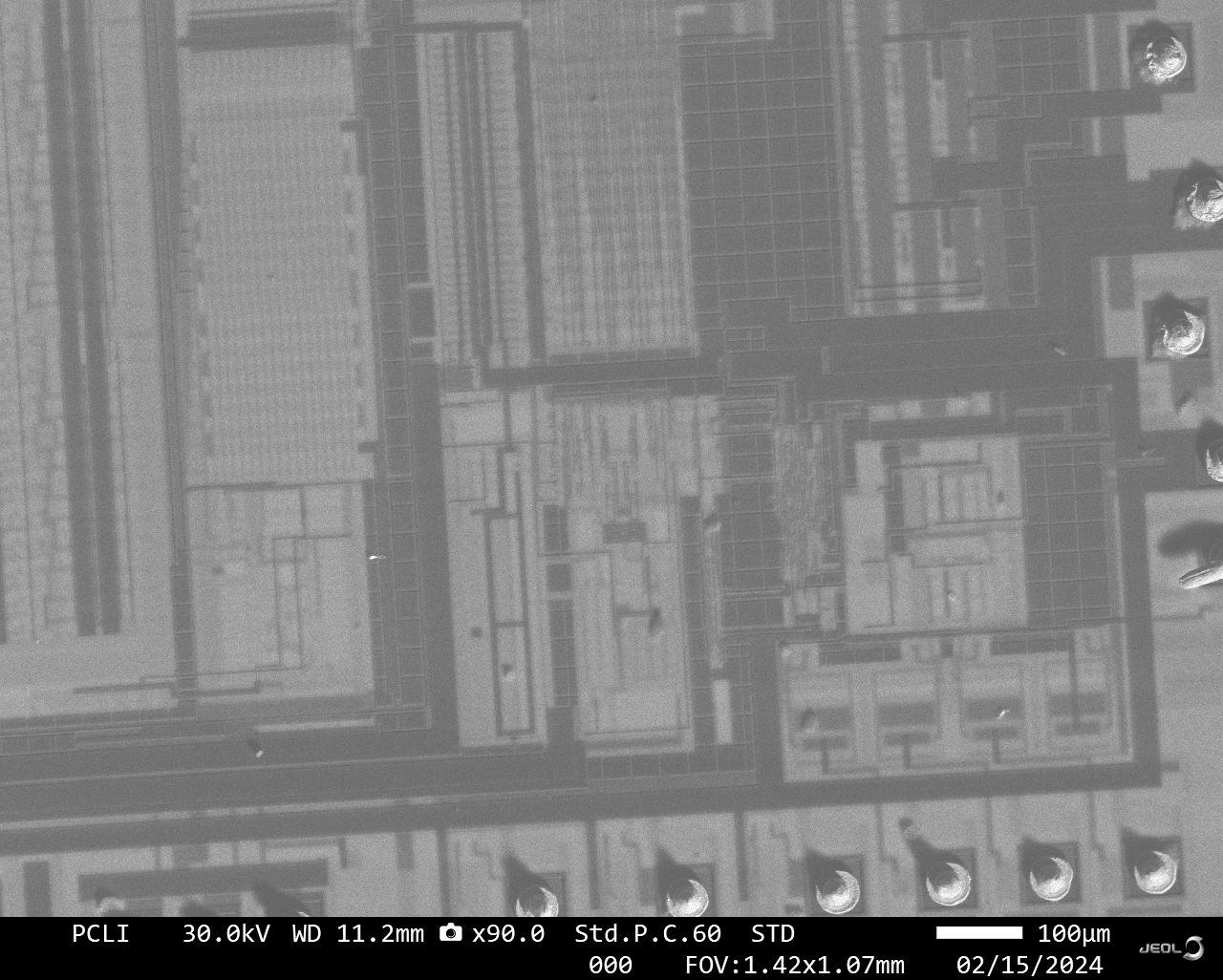
240215 -- CL image of ROI at 20 kV and 30 kV accelerating voltage. The "buried" traces seem to fluoresce very clearly. This
image is almost the inverse of the BED-C images in that the "buried" traces show up brightly, but the areas without (?) these
traces don't appear to fluoresce at all.
240215 -- False color image created using BSE (red) and CL (blue) images collected as noted above at 30 kV.
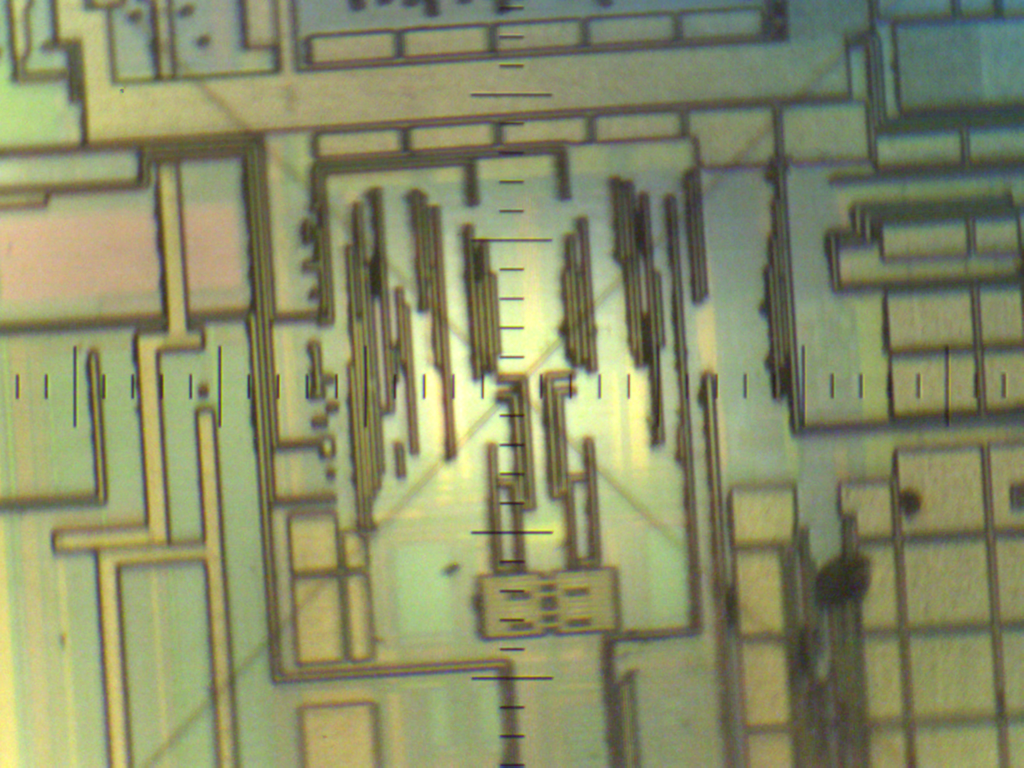
240215 -- Optical microscope (OM) image of the region of interest (ROI) taken in the same location (but different magnification) as
SEM images above. Traces can clearly be seen below the surface in visible light, but the magnification is limited. Note that the
fine demarcations on the reticle are 10 microns wide.
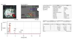
240215 -- Summary of EDS point analyses performed at a few locations in the lower right portion of the sample as viewed in the
photos shown above in the Introduction. From these I determined that Si, Al, Ti, Cu, and W seem to be elements that are worth
mapping.
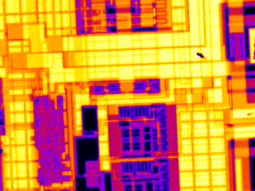
240215 -- RGB composite image of Al (red), Ti (green), and Si (blue) EDS maps. Although W and Cu were detected in point analyses,
they don't really show up in the EDS beam maps over the ROI collected over the few minutes that EDS images were made. Seems
like the traces are basically made of Ti and Al.
WDS maps were collected over approximately 5 hours with the spectrometer confguration listed below. The map resolution was
constrained by a 100 ms dwell time needed to detect the Cu Ka1 peak using 30 kV and a 100 nA beam, a 1 micron pixel step size, and
my desire to finish the maps by 5 pm. In retrospect, this time constraint never made any sense, and at the time of writing, I've
started an over-the-weekend map of the whole sample.
SP1 / PET / Si
SP2 / PET / Ti
SP3 / LiF / W? (La1)
SP4 / LiF / Cu?
SP5 / TAP / Al
240215 -- Si.
240215 -- Al.
240215 -- Ti.
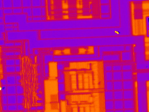
240215 -- RGB composite image of Al (red), Cu (green), and Ti (blue) WDS maps. In general, the WDS maps look excellent, and
these three elements all seem to be present in the traces with varying amounts in different locations. It looks like the Al
traces are closer to the surface, but that could just be because the Al X-rays are attenuated more easily by the sample matrix.
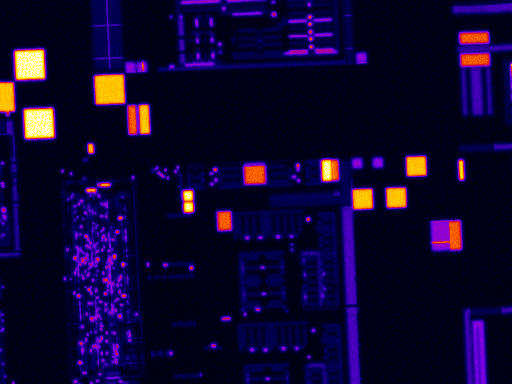
240215 -- False color WDS map of W La1. W was the most interesting element that I mapped because it clearly was present in a
limited number of locations (as opposed to being present in every trace).
240215 -- False color WDS map of Cu Ka1. Cu is mostly interesting for pedagogical reasons: it's a great example of a map that
is near what I would consider to be the detection limit (WDS peak is visible at ~3x the background standard deviation, not shown).
The map also seems to confirm something that I noticed in my random smattering of EDS spectra -- that Cu is concentrated in a
couple of places where W is also present.
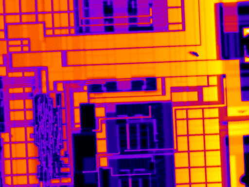
240215 -- RGB composite image of Cu (red), Ti (green), and W (blue).
After a relatively fast map of the chip (above), I decided to try mappng the whole thing over the weekend. Because of the
high dwell time needed to see Cu at my chosen beam power (100 nA?), I would only be able to get a 3-micron-wide pixel
in a 60-hour time interval.
240217 -- SEI.
240217 -- BED-C.
240217 -- PCLI.
240217 -- Si.
240217 -- Al.
240217 -- Cu.
240217 -- Ti.
240217 -- W.
240217 -- RGB composite image of Cu (red), Ti (green), and W (blue).
.bmp)
.bmp)
.bmp)
.bmp)
.bmp)